US $157,500.00
| Condition | Used
:
An item that has been used previously. The item may have some signs of cosmetic wear, but is fully operational and functions as intended. This item may be a floor model or store return that has been used. See the seller’s listing for full details and description of any imperfections.
|
| Seller Notes | “Deinstalled and crated by manufacturer. Was on Maintenance Contract.” |
Directions
Similar products from Other Semiconductors Production Tools
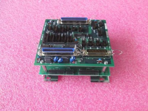
Nikon OFLNK-3 4S007-565-1B & 4S013-124 Board

Nikon 4S015-046 C NK386SX PCB Board
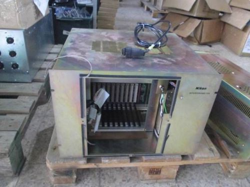
Nikon Interferometer Rack w/ Power Supply Working!
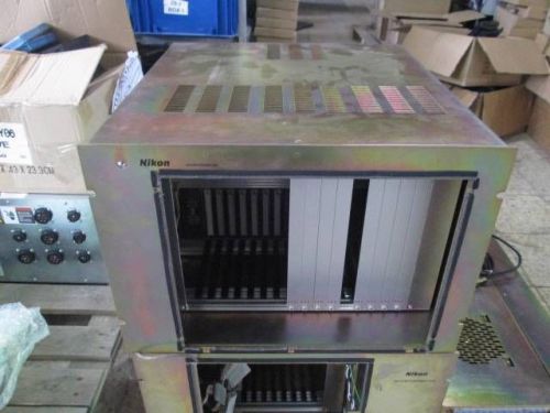
Nikon Interferometer Rack 4S018-039 w/ Power Supply Working!
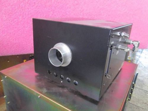
Nikon KXA46476 / T-KXA464760305
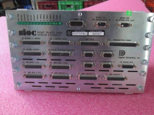
Sioc Post Plate 2000 Novellus 01-130508-00 02-8130510-00 27-053659-00 27-053660
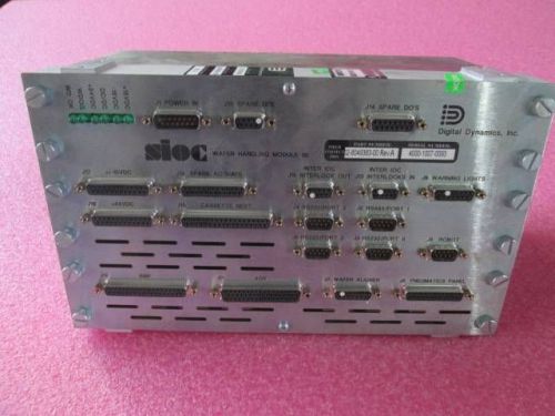
Sioc Wafer Handling Module Digital Dynamics 02-8049383 02-8049383 27-053659
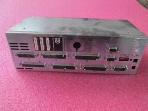
Sioc Digital Dynamics I/O Controller 27-10157-00
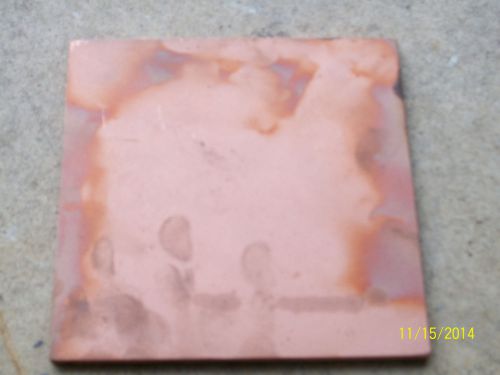
semiconductor copper anode material
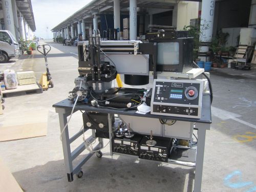
Quintel Corporation Mask Aligner ?
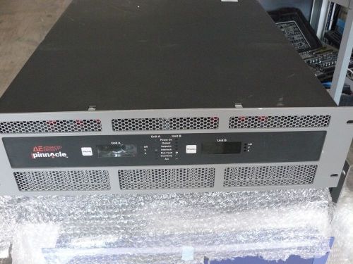
ADVANCED ENERGY 3152416-117B PINNACLE DC MAGNETRON POWER SUPPLY
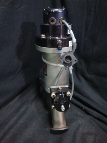
MKS Instruments, HPS, Valve/ IK 225 VLVNH F12
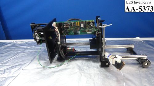
Asyst Hine Design 04630-004 Load Elevator Indexer Gasonics 94-1174 used working
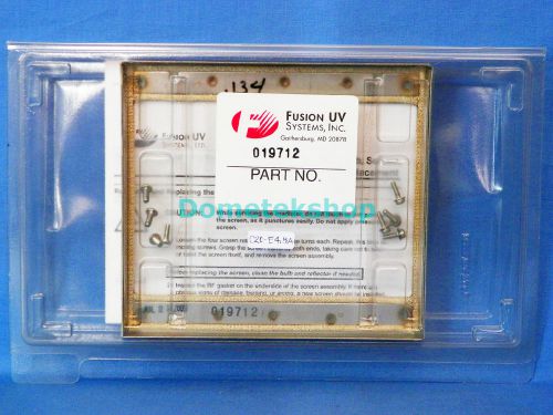
Fusion UV Systems 019712 RF Screen Kit (New)
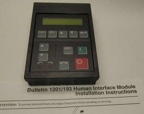
AMAT 1080-01213 CNTRL MOTOR SPEED UP-DOWN DIGITAL
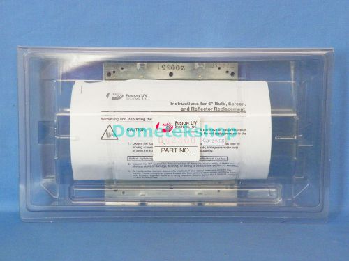
Fusion UV Systems 042306 UV Reflektor Kit
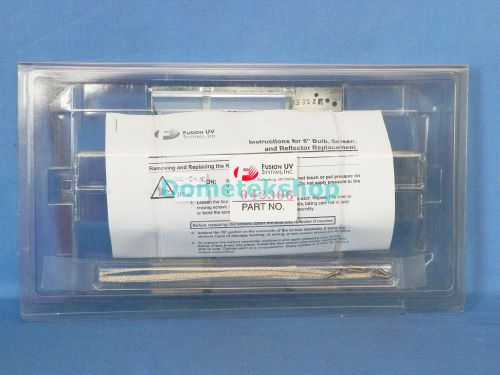
Fusion UV Systems 042306 UV Reflektor Kit (New)
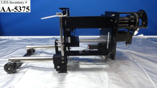
Asyst Hine Design 04630-003 Load Elevator Indexer Gasonics 94-1174 sold as is
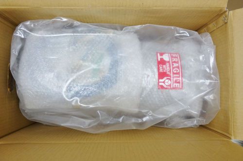
APPLIED MATERIALS 3380-01056 VESSL COMMON HEAT EXCHANGER PURGE/ FILL AMAT *NEW*
People who viewed this item also vieved
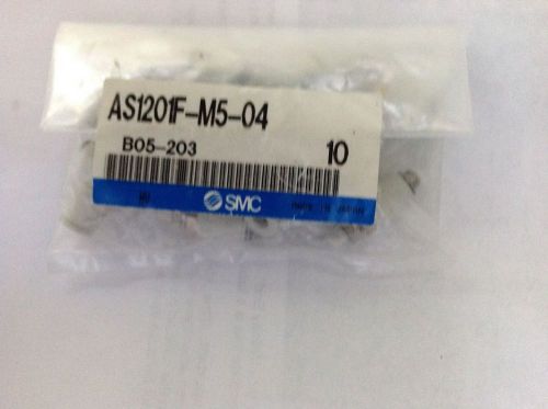
10 SMC AS1201F-M5-04 Pneumatics, New in sealed bag
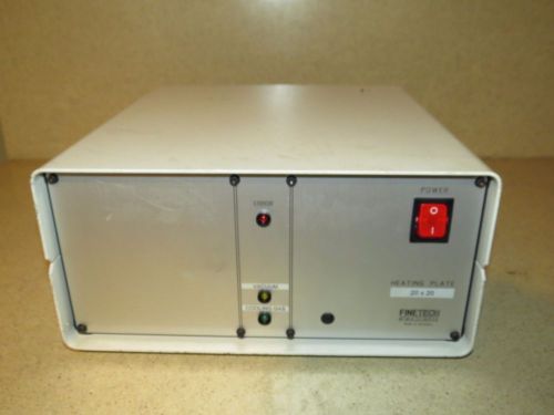
FINETECH HEATING PLATE - MODEL FA3./PC/V - 110V, 60Hz, 300W (A)
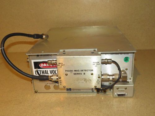
RFPP RF Plasma Products AM-20 Auto Matching Network
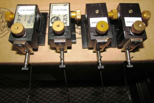
J micro Alessi Cascade XYZ Probe POSITIONERS FOR ANALYTICAL DC (QTY4)
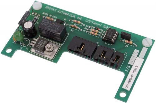
Brooks Automation 001-6843-01 PCB Circuit Board Assembly Module Plug-In 16843-01
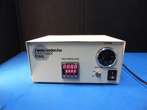
Semiconductor Equipment Corp. Model 4800 SN 4800-1499 Vacuum Temp Controller
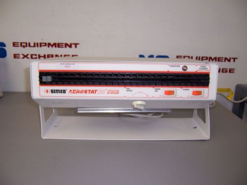
8902 SIMCO AEROSTAT XC IONIZING AIR BLOWER W/ HEAT PN: 4002612
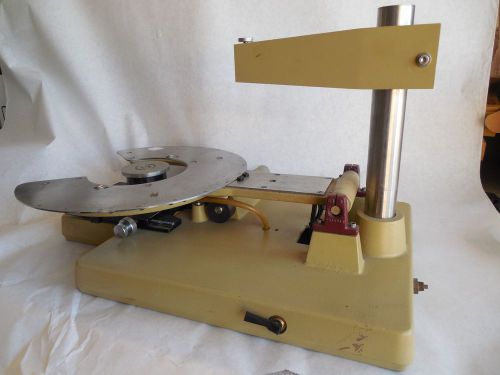
SIGNATONE Wafer Probe Station-analytic Probing Microscope Station
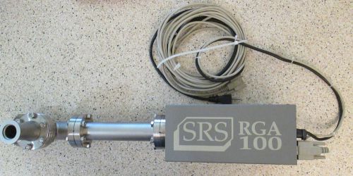
STANFORD RESEARCH SRS RGA 100 GAS ANALYZER
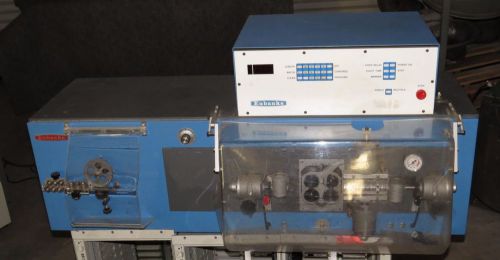
EUBANKS MODEL #2600 WIRE STRIPPER (#1119)
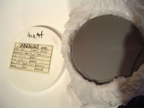
150 Westarc Silicon Wafer Matt Wafers P type 100mm ideal for Solar Cells
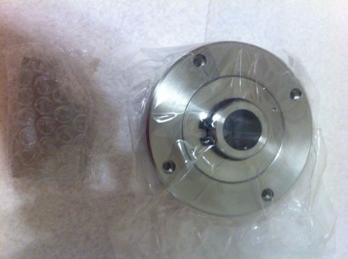
RIGAKU MAGNETIC FERO - FLUID SEAL,CV21604
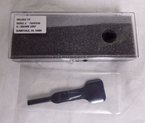
H-Square T694PKAS PEEK Vacuum Tip Wafer Handler 100 - 150 mm Length 4" (C6)
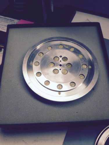
5" Ceramic porous cutting chuck used on K&S 980 Dicing saw
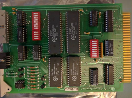
LAM RESEARCH 810-000392-001 REV D ASSY PCB SIO
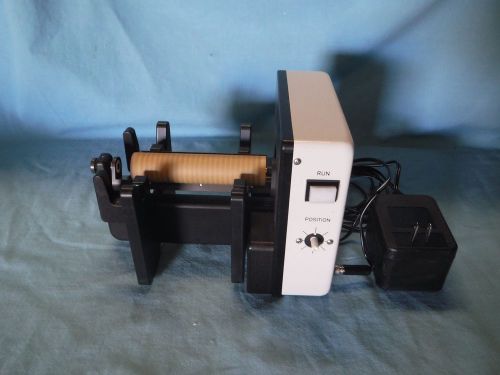
H-SQUARE AUTOMATIC WAFER 5" WAFER ALIGNER AFEZ-5AL
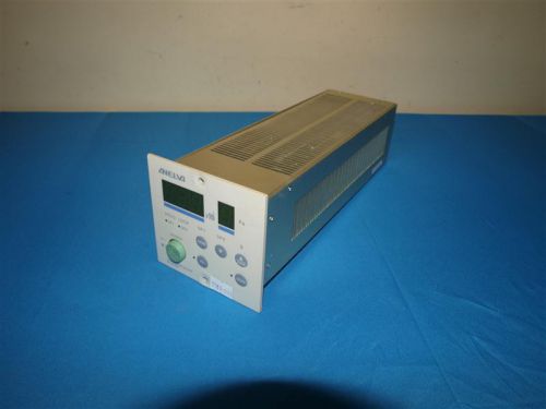
Anelva M-431HG Ionization Gauge
By clicking "Accept All Cookies", you agree to the storing of cookies on your device to enhance site navigation, analyze site usage, and assist in our marketing efforts.
Accept All Cookies